

I wanted a compact, programmable and easy to use signal source that could help me with my other projects. The widely available AD9850 and AD9851 direct digital synthesis (DDS) modules are electrically capable enough for filter sweeps, ADC checks, receiver alignment, and quick frequency-counter tests. The real challenge was whether a Raspberry Pi could drive the DDS cleanly from Linux user space in C++, without adding a separate microcontroller just to handle RESET, W_CLK, FQ_UD, and data.
The result is ad985x-raspberry-pi: a C++ control suite with both a scriptable CLI and a full-screen text user interface. It supports serial and parallel load modes, AD9850 and AD9851 including the 6x PLL mode, libgpiod v2 on Raspberry Pi, a simulation backend for development and CI, and bench validation with oscilloscope measurements.
This article walks through the practical details: hardware setup, wiring, perfboard craftsmanship, command workflow, software architecture, and real scope validation.
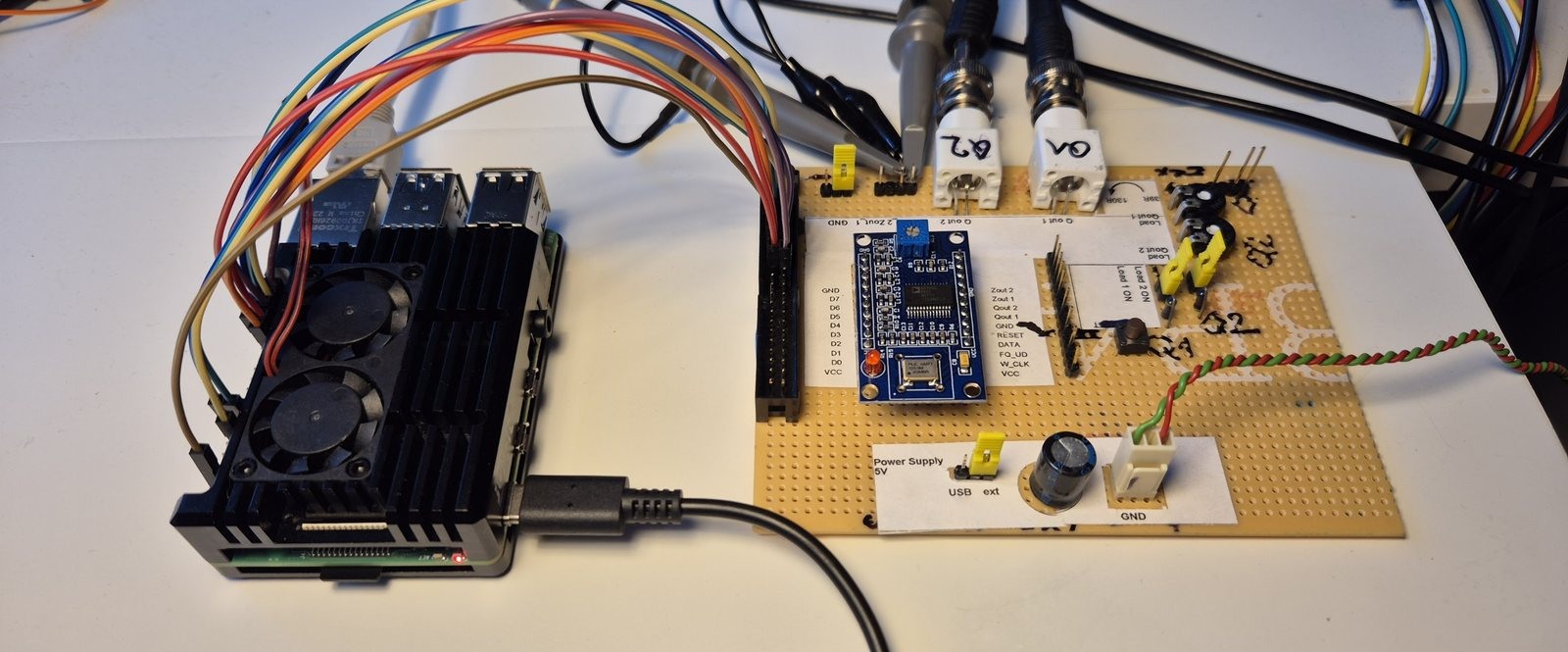
This article is the practical version of that project. It covers the electrical setup, the command-line and TUI workflow, the Linux and C++ boundaries that made the driver testable, and the scope checks that confirmed the output.
Guide to this article
- Page 1: live parallel-mode demo, DDS basics, power, wiring, and the handmade development board
- Page 2: CLI and TUI workflow at the bench
- Page 3: Linux GPIO, C++ library boundaries, static linking, and simulation
- Page 4: scope validation and current validation state
GitHub repository
The code is published as ad985x-raspberry-pi: a C++ core library, CLI, text user interface, libgpiod backend, simulation backend, and smoke tests.
Live TUI demo in parallel mode
The short clip below shows the TUI, a text user interface that runs in the terminal, driving the DDS in parallel mode while the scope follows the frequency changes. It is the quickest proof that the project is not only a driver library or a terminal UI, but a real bench tool controlling real hardware.
What the chip actually needs
The AD9850 is a direct digital synthesis chip. With the common 125 MHz module oscillator, software writes a 32-bit frequency tuning word into the device and the chip generates the corresponding output. The relationship is the one from the AD9850 datasheet:
![\[ f_{\mathrm{out}} = \frac{FTW \cdot f_{\mathrm{SYSCLK}}}{2^{32}} \qquad FTW = \mathrm{round}\!\left( \frac{f_{\mathrm{out}} \cdot 2^{32}}{f_{\mathrm{SYSCLK}}} \right) \]](https://www.embedonix.com/wp-content/ql-cache/quicklatex.com-b40d77936fed59fab2630972d44414ee_l3.png "Rendered by QuickLaTeX.com")
At 125 MHz, the tuning resolution is about 0.029 Hz per step. For this kind of bench source, the oscillator tolerance matters far more than the math.
The complete programming word is five bytes:
|
1 2 3 4 5 |
W0 = phase[4:0] << 3 | power_down << 2 | 0 << 1 | pll6 << 0 W1..W4 = FTW, most significant byte first |
That small layout drives a lot of the software. The five phase bits give 11.25 degree phase steps. Bit 2 powers the output down. Bit 1 must stay zero because it selects factory test behavior. Bit 0 is the 6x reference multiplier on the AD9851, but on an AD9850 it is another bit that should not be set. Because the chip has no readback, the program has to keep dangerous W0 combinations away from the pins before the load starts.
The chip accepts the word in either of two ways:
- Parallel mode presents five bytes on D0 through D7, pulsing W_CLK once per byte, then FQ_UD once to latch the word.
- Serial mode shifts forty bits on D7, pulsing W_CLK once per bit, then FQ_UD once to latch the word.
For my setup, serial mode is the useful default. It needs only DATA, W_CLK, FQ_UD, and RESET as driven signals. D0, D1, and D2 only need the 1, 1, 0 strap pattern during serial-mode entry. On the bench, the tool can hold that pattern with Raspberry Pi internal pulls; on a PCB, the mode pins should be hard-strapped instead.
Wiring and power first
Power warning: Raspberry Pi GPIO is not 5 V tolerant. For this tested module, 3.3 V operation worked and keeps the DDS logic interface directly compatible with Raspberry Pi GPIO. If a module must run from 5 V, do not connect the Pi GPIO pins directly; use proper 3.3 V-to-5 V buffering or level shifting.
The easy mistake is to treat every AD9850 module like the same 5 V Arduino-style board. For this prototype I powered the module from the Raspberry Pi 3.3 V rail, with a common ground and a supply capable of at least 150 mA. The tested board uses an active 125 MHz oscillator can marked PLE SM77 125.0M 2GM6R, which appears to be from a 3.3 V-capable CMOS oscillator family. That explains why this module operated correctly at 3.3 V in the bench tests.
That result is not a guarantee for every low-cost AD9850 board. Some modules may use 5 V oscillator cans or layouts that are not reliable at 3.3 V, and the AD9850 datasheet is more conservative at 3.3 V than at 5 V for maximum reference-clock operation. For production hardware, verify the exact oscillator and module, use a known 3.3 V-compatible 125 MHz oscillator, or run the DDS module at 5 V with a suitable HCT/AHCT buffer or another proper level-shifting solution between the Pi and the DDS pins.
The default serial wiring is deliberately small:
| signal | BCM GPIO | 40-pin header pin | serial-mode role |
|---|---|---|---|
| D0 | 5 | 29 | prototype: internal pull-up; PCB: 10 kΩ to 3.3 V |
| D1 | 6 | 31 | prototype: internal pull-up; PCB: 10 kΩ to 3.3 V |
| D2 | 12 | 32 | prototype: internal pull-down; PCB: 10 kΩ to GND |
| D7 / DATA | 26 | 37 | serial data |
| W_CLK | 17 | 11 | shift clock |
| FQ_UD | 22 | 15 | latch strobe |
| RESET | 23 | 16 | hardware reset |
| VDD | 3V3 | 1 or 17 | module supply |
| GND | GND | 6, 9, 14, 20, 25, 30, 34, or 39 | common ground |
Parallel mode uses D0 through D7 as driven outputs, plus the same W_CLK, FQ_UD, and RESET lines. That path is now hardware validated too. I would still treat the first run on any new wiring setup as a scope session, but parallel mode is no longer only a simulation result. If a PCB is serial-only, the D0, D1, and D2 GPIO connections are optional/debug-only; hard straps are the deterministic choice. Keep those GPIO connections only if the board also needs to support parallel-load mode or bench reconfiguration.
For parallel-load wiring, keep the same W_CLK, FQ_UD, RESET, 3.3 V, and GND connections, then wire the full data bus. The additional data pins are:
| extra parallel signal | BCM GPIO | 40-pin header pin |
|---|---|---|
| D3 | 13 | 33 |
| D4 | 16 | 36 |
| D5 | 19 | 35 |
| D6 | 20 | 38 |
D0, D1, D2, and D7 are already listed in the serial table above; in parallel mode they become driven data lines instead of straps or serial DATA.
The craft in a perfboard development board
A perfboard development board does not have to look temporary. For this kind of one-off instrument adapter, the goal is not only to make the circuit work once. The goal is to make it inspectable a week later, after the jumper colors and bench notes have stopped being fresh in your head.
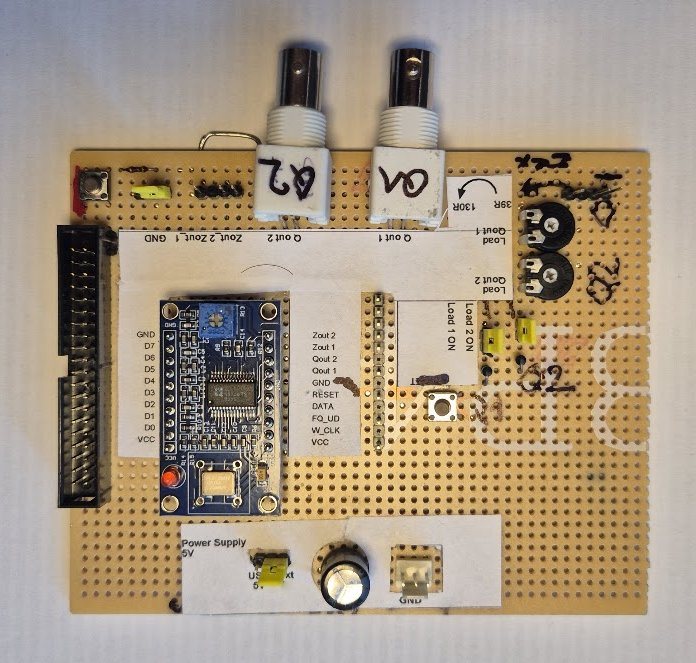
The baseboard is not required, but it made the validation less annoying. Labeled headers matter when there are enough signals to be off by one row. The reset button and BNC connectors also made it easy to separate wiring mistakes from driver behavior.
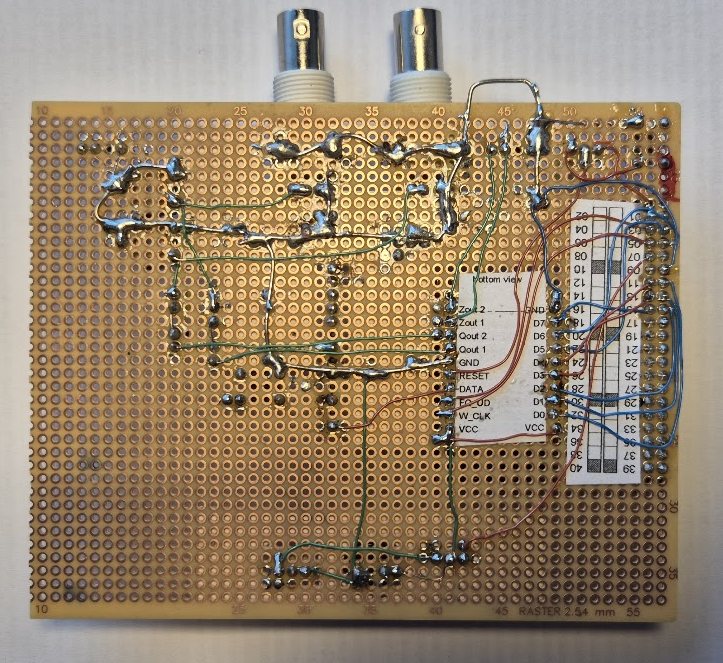
That is why the underside matters. Short point-to-point routes, visible signal grouping, labeled headers, and enough mechanical strain relief turn a quick prototype into a usable bench fixture. It is slower than plugging the module into a breadboard, but it pays back the first time a scope trace looks wrong and you can follow W_CLK, FQ_UD, RESET, and the data bus by eye. There is a real craft to making perfboard wiring clean enough that it becomes part of the documentation.
The hardware is now ready. Page 2 moves from the board to the operator workflow: the CLI for scripts, the TUI for live bench work, and the response lines that make both usable during probing.