

Part 4 of 4. Page 3 covered the C++ core library, CLI/TUI separation, Linux GPIO details, and simulation. This final page shows what the hardware did on the scope, including a live parallel-mode demo.
What the scope confirmed
The hardware validation loop was straightforward: send commands to the Pi over SSH, measure all four outputs on a scope, and compare the observed result with the command response. Two channels watched the sine outputs and two watched the comparator square outputs.
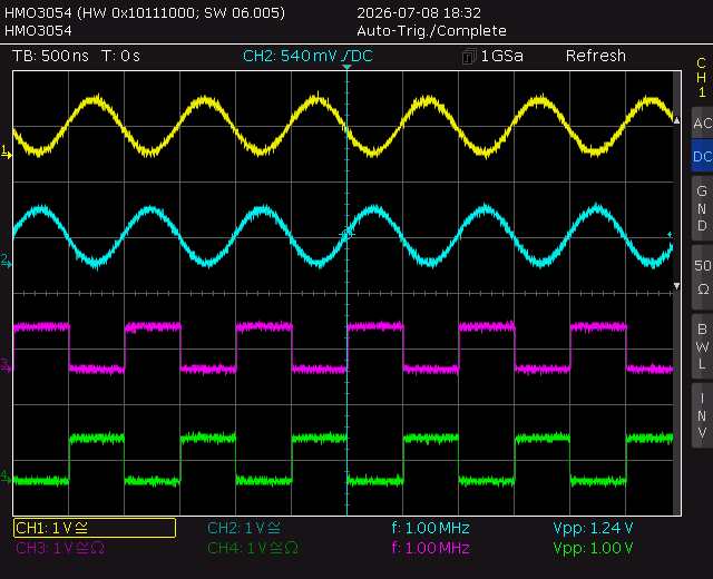
| Programmed output | Scope count on square output | Sine amplitude |
|---|---|---|
| 1 MHz | 1.00000 MHz | about 1.20 Vpp |
| 5 MHz | 5.000000 MHz | about 1.08 Vpp |
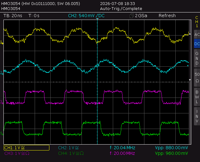
| 12.5 MHz | 12.50000 MHz | about 0.96 Vpp |
| 20 MHz | 20.000000 MHz | about 0.92 Vpp |
The square outputs were the best place to count frequency. The sine outputs were better for checking amplitude roll-off and general analog behavior. The gentle drop in sine amplitude toward 20 MHz is expected from the DDS DAC response and the module output filter.
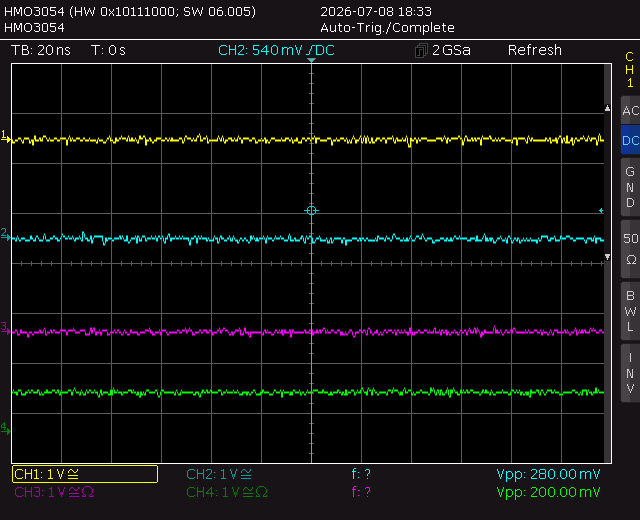
Power-down was also checked directly. Setting the power-down bit collapsed all four outputs to the noise floor. Clearing it restored the previous frequency, which matches the chip behavior and the tool’s cached-state model.
Current validation state
The current bench work now covers the serial AD9850 path, the parallel AD9850 path, and AD9851 operation including the 6x PLL profile. It also proves the shared CLI/TUI command engine, stream playback, reset recovery, power-down behavior, and simulation path.
The remaining caveat is not an untested driver mode. It is normal bench discipline: every new wiring setup should still get a first-run scope check on W_CLK, FQ_UD, and the output, and the output quality is still bounded by the specific DDS module, reference oscillator, comparator threshold, and filter network.
For my use case, the useful part is not only that the Pi can program the DDS. It is that the same tool can be used from a script, from the TUI, or in simulation, and the byte order is tested before I ever connect the module.